
Nanoscale Fabrication
We build nanometer scale devices with precise control provided by state-of-art fabrication tools. We also develop fabrication tools in our lab, such as electromigration technique, to go beyond the resolution of ebeam lithography to make devices down to atomic scale. This capability, combined with our nanomaterial synthesis, provides a powerful platform to investigate quantum effects in spatially confined materials. This understanding not only reveals interesting physics in low dimensions but also guides new materials and new devices design. In return, we can implement this understanding with our fabrications capability to create novel electronic or opto-electronic devices for applications.

Dual gated graphene device fabricated using CVD graphene. We fabricate hundreds of devices with high high mobility. This high quality devices enables photocurrent measurement in graphene pn junction, revealing hot carrier behavior in graphene.
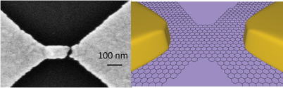
Ultra-small plasmon enhanced photo-detector by coupling gold break junction with graphene nanoconstriction (left). The graphene constriction is too small to be seen directly under scanning electron microscope (SEM), and we show it schematically (right).
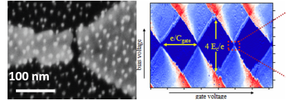
Single electron transistor (SET) device made by single metallic nanoparticle (Au, Pd, or Pt). We can functionlize the break junction surface and bridge the nanometer scale gap by a chemically synthesized metal nanopartcile. The SEM (left) show a typical device and the differential conductance measurement as a function of gate voltage and bias exhibits typical Coulomb diamond pattern, a result of Coulomb blockade (electrons have to tunnel through one by one).